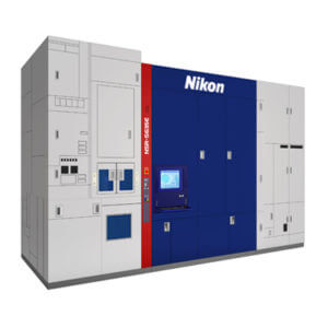
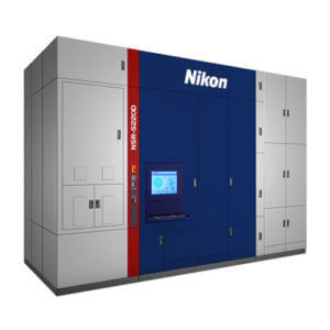
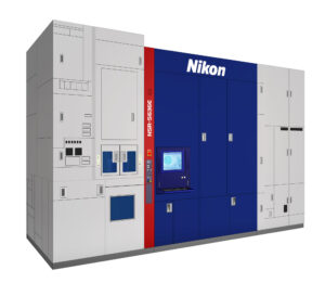
 Introducing the NSR-S636E ArF Immersion Scanner
The NSR-S636E is an immersion lithography scanner for critical layers that delivers superior overlay accuracy and ultra-high throughput.

March 28, 2024
Nikon Corporation is proud to announce that it has earned Intel’s EPIC Distinguished Supplier Award.
July 9 – 11, 2024
Join us at Booth #1032 in the South Hall and learn how our advanced lithography and inspection solutions can support you path to the future!
We invite you to explore a Career at Nikon Precision or Nikon Research Corporation of America! To learn more about our current open positions, click below.
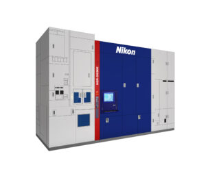
The NSR-S636E is an immersion lithography scanner for critical layers that delivers superior overlay accuracy and ultra-high throughput.
March 28, 2024
Nikon Corporation is proud to announce that it has earned Intel’s EPIC Distinguished Supplier Award.
![]()
July 9-11, 2024
Join us at Booth #1032 in the South Hall and learn how our advanced lithography and inspection solutions can support your path to the future!
We invite you to explore a Career at Nikon Precision or Nikon Research Corporation of America! To learn more about our current open positions, click below.