- Home
- About Us
- Products and Technology
- Support and Training
Satisfying semiconductor makers’ challenging inspection requirements
In addition to delivering steppers and scanners for cutting-edge semiconductor applications, Nikon also offers advanced AMI-5700 semiconductor inspection systems. Nikon leverages over 100 years of optical design and manufacturing expertise to deliver automatic macro inspection (AMI) systems to meet the most challenging inspection requirements of today’s IC makers.
Comprehensive inspection solutions for coating issues, defocus, particles and more
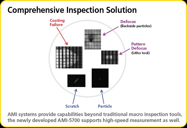
AMI systems capture wafer images and then use artificial intelligence (AI) image processing to compare those images with previously learned defect-free wafer images to identify defects. The evaluation judgment can identify the number of defects or defective chips, perform auto defect classification (ADC), and report defects’ shapes, etc. AMI-5700 systems can detect particles (foreign materials) as small as 5 μm, scratches and uneven resist coatings. In addition – they can detect a variety of pattern defocus conditions that are typically beyond the capabilities of traditional macro inspection tools.
Through the successful integration of a variety of Nikon proprietary optical systems including diffraction, polarization and pattern edge roughness techniques, AMI-5700 tools can successfully detect a multitude of defect types that are extremely difficult or time-consuming for other inspection systems to capture. AMI-5700 systems deliver augmented image quality compared to earlier models due to reduced chromatic aberrations made possible by the newly developed optical system and enhanced collection mirror.
Optimal sensitivity for immersion lithography and advanced nodes
The Nikon AMI diffracted light detection system detects pattern variations along the Z-axis including focus error as well as coating abnormalities with ultra-high sensitivity. In addition, accurate recognition of the diffracted light only from the top pattern layers is possible, allowing defects in underlying patterns to be differentiated. The AMI-5700’s new mirror tilting mechanism contributes to reduced underlayer noise and better detection of changes in the top layer.
Deliver ultra-high throughput inspection of entire wafer surface
AMI systems capture the entire wafer surface in a single image, enabling 100% lot inspection with ultra-high throughput. The enhanced 5700 can process 180 wafers/hour or more, and provides an additional 3rd wafer carrier load port to streamline manufacturing operations.
AI-driven image processing and sophisticated defect classification enhance inspection capabilities
Nikon’s proven image processing technology, driven by AI is applied for intelligent device inspection. Proprietary learning functions quantify acceptable “good wafer image” results for each process, providing the flexibility to adapt to diverse processes and provide stable inspection output. The AMI systems also support ADC and operators can specify their rework criteria within specific recipes to automate rework judgment. The AMI systems’ automatic recipe creation function is user-friendly and requires minimal experience for programming.
Supports CD, film thickness and focus measurement
The industry-leading AMI-5700 system can be equipped with an innovative add-on high-speed measurement function that supports CD, film thickness and focus measurements at speeds surpassing those of other methods. This enables the AMI-5700 to deliver superior throughput of 180 wafers/hour even when performing diffraction and scattering batch inspection of the entire wafer. The innovative AMI-5700 not only inspects, but also measures wafers and detects defects.
Nikon is committed to providing industry-leading inspection solutions like the AMI-5700 that enable customers to advance semiconductor manufacturing and support the digital transformation