- Home
- About Us
- Products and Technology
- Support and Training
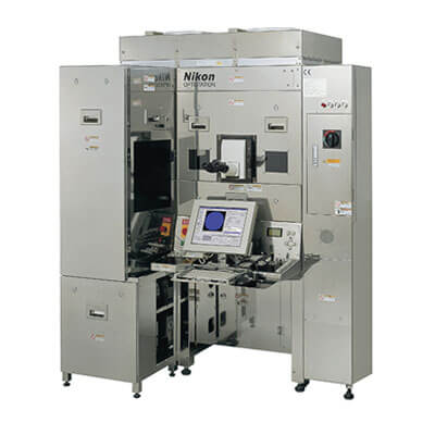
Satisfying semiconductor makers’ challenging inspection requirements
In addition to delivering steppers and scanners for cutting-edge semiconductor applications, Nikon also offers a suite of advanced semiconductor inspection systems. Nikon leverages over 100 years of optical design and manufacturing expertise to deliver OPTISTATION-3000 series inspection systems to meet the most challenging post-develop and post-etch inspection requirements of today’s IC makers.
Provide advanced micro/macro inspection capabilities in compact and flexible design
OPTISTATION-3000 series products are available to meet a variety of fab configurations and wafer handling requirements. The OST-3000 is a cost-effective single load port solution available for 200 mm or 300 mm wafer inspection applications. Loading a 200 mm cassette adapter to the OST-3000 enables the combined transfer of 200 and 300 mm wafers on a single unit. The OST-3000’s load port’s auto recognition of cassettes and intelligent shared-parts design eliminates the need for time-consuming wafer size adjustments and maximizes equipment uptime.
Nikon also offers the OST-3100 single load port and OST-3200 dual load port systems to meet a variety of fab layout and automation handling requirements for 300 mm wafers (200 mm capabilities optional). Overhead transfer (OHT) and other automatic transfer systems are supported as well. Nikon understands that there is often variability in production wafer flatness, and the OPTISTATIONS’ high-speed, multi-axis robots and proprietary handling systems fully support the transfer of warped wafers.
Industry-leading optics enable images with high contrast and minimal flare
OPTISTATION-3000 series systems incorporate renowned Nikon CFI60-2 objectives, which produce excellent images with high contrast and reduced flare. The OST systems also provide brightfield and darkfield micro inspection modes. Their darkfield inspection signal-to-background noise ratio is 3x higher than previous generation systems, thereby significantly improving imaging.
Long working distances optimize wafer inspection capabilities
OPTISTATION-3000 series systems enable micro inspection across the total magnification range of 25x to 1,500x. The long working distances throughout this range ensures safer wafer inspection and also suppresses problematic image skipping that sometimes can occur when switching from low to high magnifications. The well-established OST design enables inspection systems having superior performance and stability, combined with high resolution.
Multiple macro inspection modes and high performance illuminators enhance defect detection
Surface Macro, center wafer backside Macro, and perimeter wafer backside Macro inspection functions are all possible with OST-3000 series systems. Rotation speed and tilt angle during macro inspection are controlled manually by the OST-3000 using a joystick. The advanced OST-3100 and 3200 systems’ automated and motorized functions are easily controlled by a touchscreen, and their observation settings such as aperture and light intensity can be preset according to objective magnification and substrate layer to optimize inspection performance. The OST-3100 and 3200 systems also include the proprietary Nikon wide illuminator (WIL-100) and line illuminator (LIL-100), which were specially developed to detect a variety of process defects, particles and scratches.
Proven platform delivers optimal uptime and productivity
OPTISTATION-3000 systems are built upon a highly robust and stable platform to maximize fab performance and productivity. In addition, OST-3100 and 3200 tools integrate sophisticated environmental chambers and fan filter units to prevent problematic particle contamination. Nikon continues to expand inspection and review capabilities, and host communication and other functions are also available for OPTISTATIONS to meet customers’ evolving inspection requirements.
Objectives
| Magni- fication | Numerical Aperture | Working Distance (mm) | Type |
|---|---|---|---|
| 5X | 0.15 | 18 | TU Plan Fluor BD |
| 10X | 0.30 | 15 | TU Plan Fluor BD |
| 20X | 0.45 | 4.5 | TU Plan Fluor BD |
| 50X | 0.80 | 1.0 | TU Plan Fluor BD |
| 100X | 0.90 | 1.0 | TU Plan Fluor BD |
| 150X | 0.90 | 1.5 | TU Plan Apo BD |
Enhances wafer micro inspection safety and minimizes image skipping.
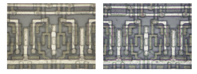
CFI60-2 objectives produce excellent images with high contrast and reduced flare.