Nikon Precision | USA & Europe | Nikon Global Site

Products and Technology

Products and Technology

Nikon continues to expand its vast portfolio of lithography systems. The diverse needs of today’s semiconductor manufacturers are met with products like the recently announced NSR-2205iL1 5x reduction i-line stepper. These are coupled with ultra-high productivity dry NSR-S322F ArF and NSR-S220D KrF scanners. The industry-leading NSR-S636E and NSR-S625E scanners also satisfy advanced immersion lithography requirements and are integrated with the pioneering inline Alignment Station (iAS). iAS capabilities can be extended to other scanners in the fab with the Litho Booster Standalone Alignment Station. Litho Booster delivers shot-by-shot feed forward corrections and provides an open platform for expanded overlay, autofocus, and process control solutions.

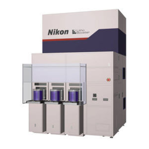
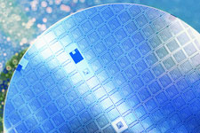
In addition, Nikon offers a line-up of advanced semiconductor inspection equipment including OPTISTATION and Automated Macro Inspection (AMI) systems, as well as specialized illumination systems for image sensor inspection. Nikon has also specially developed lithography and metrology solutions for MEMS, LED, and packaging applications. MEMS steppers deliver maximum yield at the lowest possible cost, as well as the large depth of focus and backside alignment capabilities that are vital for these growing markets.

Nikon. Technology to Do More.

Nikon Products and Technology
Immersion and Multiple Patterning

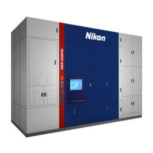
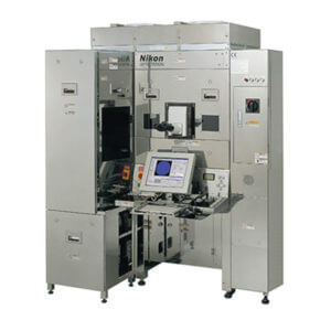
Industry-leading scanners satisfy the stringent requirements for immersion and multiple patterning applications.

Nikon Products and Technology NSR-S220D Deep UV
Deep UV

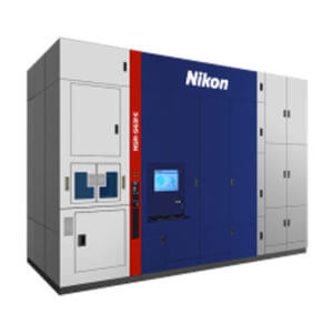
DUV scanners play an essential role in semiconductor manufacturing, and Nikon provides a variety of systems to meet chipmakers’ production requirements.


Alignment Stations
Alignment Stations

Standalone Alignment Station delivers shot-by-shot feed forward corrections to maximize yield.


Semiconductor Inspection Systems

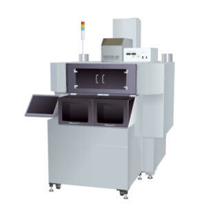
Nikon offers a suite of After Develop (AD) and After Etch (AE) inspection solutions and specialized illumination systems for image sensor inspection.


i-Line

Provide excellent performance and cost-effective solutions for diverse applications.


Nikon Products and Technology
Steppers and Metrology Solutions for MEMS Markets

Nikon continues to expand this product line to satisfy the unique lithography requirements of MEMS, LEDS, back-end applications and more. Dual-side overlay metrology solutions are available as well.