- Home
- About Us
- Products and Technology
- Support and Training
Delivers industry-leading KrF performance and productivity through Streamlign platform innovations
The semiconductor industry is transitioning to development and high volume manufacturing of next-generation process devices, with the most critical layers exposed using immersion scanners with multiple patterning. As design rules become more challenging and to contain costs for non-immersion layers, KrF scanners must deliver ultra-high productivity with overlay accuracy comparable to immersion systems, as well as exceptional system stability and matching capabilities.
The Nikon NSR-S220D is the industry-leading KrF scanner for high volume manufacturing. It combines the proven Streamlign platform with continuous technology advancements to satisfy the requirements of the most demanding KrF layers.
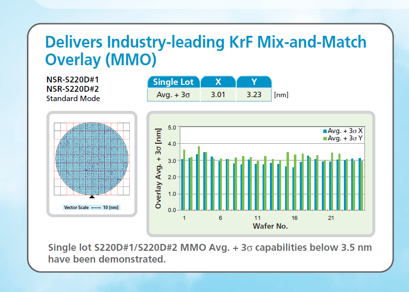
Enables superior yield with overlay accuracy down to 2.5 nm
The Nikon DUV S220D scanner utilizes the proven Bird’s Eye Control system, which uses laser encoders along with conventional interferometers to accurately determine wafer position time after time. This is coupled with enhanced lens distortion and reticle thermal management solutions which improve focus control.
In addition, the S220D incorporates an improved autofocus light source, and Phase Shift Focus Monitor (PSFM) across wafer focus control < 20 nm (including edge shots) has been achieved.
Maximizes manufacturing flexibility with mix-and-match overlay capabilities to 5 nm
Mix-and-match overlay (MMO) is vital for advanced applications, and compensation functions that adjust the grid and distortion of one scanner to another are essential for heightened matching performance. The S220D supports a multitude of advanced shot distortion correction capabilities provided by Dynamic Matching Adjustment Control. These cutting-edge compensation functions optimize performance for the most stringent mix-and-match requirements, even under extremely high exposure dose situations.
The Nikon NSR-S220D successfully enhances scanner matching capabilities and production flexibility, delivering (NSR-S220D#1 to S220D#2) MMO performance below 6 nm. This is improved to 5 nm with the High Precision Mode (HPM) option. Mix-and-match overlay between immersion and dry scanners is of particular importance in today’s manufacturing environment. MMO data collected using the NSR-S631E immersion scanner for the first print, and the S220D for the second print showed multi-wafer MMO Avg. + 3σ capabilities below 4 nm.
Ensures excellent imaging with enhanced 0.82 NA lens and sophisticated control solutions
The S220D features an enhanced 0.82 numerical aperture projection lens to enable resolution of 110 nm or better with optimal CD uniformity. Superior materials and proprietary manufacturing technology provide a virtually perfect lens that is essentially flare free and has the industry’s lowest aberration levels. The S220D delivers low lens distortion, and employs an advanced lens controller and reticle cooling system.
The NSR-S220D also enables a number of advanced tool control solutions, which further enhance tool stability and on-product performance. The Zeroing Autofocus function performs automated periodic machine calibration that improves scanner stability with machine-specific autofocus corrections. Similarly, the Zeroing XY function can perform automated periodic machine calibrations and machine-specific grid corrections to further enhance overlay stability.
Provides optimal affordability with throughput up to 250 wafers per hour
Chipmakers will utilize KrF lithography as much as possible to balance multiple patterning costs. Therefore, S220D throughput is an essential factor in making less-critical processes cost effective for manufacturing. The NSR-S220D employs state-of-the art dry sequencing, and its wafer stage uses optimized scan speed and acceleration capabilities to reduce exposure time. In addition, the Stream Alignment wafer mapping system utilizes multiple alignment microscopes (Five-Eye FIA) and a wide area autofocus sensor (Straight Line Autofocus) that spans the wafer to pre-scan the substrate during loading−dramatically reducing wafer overhead time. Together, these innovations enable throughput ≥ 230 wafers per hour (WPH) using 96 exposures/wafer. Throughput is further increased to 250 wafers per hour or more with the High Throughput Mode (HTM) optional configuration.
| Wavelength (nm) | 248 |
| Lens-NA | 0.82 |
| Exposure Area (mm) | 26 x 33 |
| Reduction Ratio | 1/4 |
| Resolution (nm) | ≤ 110 |
| Mix-and-Match Overlay (nm) | ≤ 6 (≤ 5.0 with HPM or ≤ 7.0 with HTM) |
| Throughput: | |
| 300 mm (96 exp fields) | ≥ 230 (≥ 200 with HPM or ≥ 250 with HTM) |
| Wafer Size (mm) | 300 |