- Home
- About Us
- Products and Technology
- Support and Training
Deliver i-line capabilities with resolution ≤ 1.2 µm
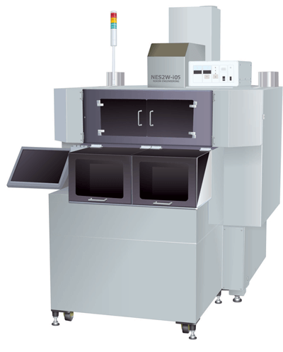
Nikon recognizes that i-line requirements are becoming increasingly challenging, and the NES1W-i05/NES2W-i05 steppers accommodate i-line resist processing and deliver resolution capabilities below 1.2 µm, with champion data down to 1.0 µm demonstrated. The NES1W-i05 and NES2W-i05 systems fully satisfy the needs of leading-edge MEMS manufacturing.
Accommodate challenging process requirements with 10 µm depth of focus
These MEMS steppers utilize a 0.10 to 0.20 variable numerical aperture projection lens design with 2.0x reduction that was developed to address the unique process challenges presented by these specialized i-line applications. The NES1W-i05/NES2W-i05 systems enable up to 10 µm depth of focus, and their advanced autofocus systems provide die-by-die autofocus capabilities that further increase yield for these difficult processes.
Maximize productivity with throughput beyond 75 WPH
The NES1/2W-i05 handling system employs a newly developed edge grip design that works well with TAIKO® and other thin wafers, and the verneuil chuck can utilize non-contact delivery as well as traditional handling. The chuck design also enables dual-sided non-contact exposure. The NES1-i05 system can process more than 75 6” wafers per hour.
Enhance mix and match with NSR steppers using 22 mm field size
The NES1W-i05/NES2W-i05 make use of advanced lens technology to enable the same 22 mm x 22 mm exposure field as traditional 5x reduction steppers, simplifying mix-and-match applications while boosting productivity. To further ease matching and reticle design, it is also possible to use the same alignment marks (FIA X/Y simultaneous marks) on these systems as on traditional NSR steppers.
Deliver excellent overlay performance
Problematic effects such as wafer deformation and process-induced shrinkage can be challenging for some applications; however, the NES1W-i05 and NES2W-i05 employ enhanced global alignment (EGA) to optimize overlay accuracy to 0.30 and 0.35 µm respectively for the large 22 mm field. EGA functions by utilizing multiple alignment marks across the wafer to ensure best fit alignment and thereby compensate for rotation issues or process-induced deformations. Pattern Matching Alignment capabilities are also available to provide increased flexibility for reticle design.
Support backside alignment to 0.8 µm
Customers may also choose to add on backside alignment functionality to enable precise alignment of 0.8 µm and below to marks located on the backside of the wafer surface. The newly developed backside alignment system incorporates both direct and infra-red alignment capabilities to optimize performance.
| Wavelength (nm) | 365 |
| Lens-NA | 0.10 to 0.20 variable |
| Exposure Area (mm) | 22 mm square |
| Reduction Ratio | 1/2 |
| Resolution (µm) | 1.2 |
| Depth of Focus (µm) | 10.0 |
| Overlay Accuracy (µm) | 0.30 |
| Throughput | NES1W-i05: 150 mm – 76 WPH NES2W-i05: 200 mm: 42 WPH |
| Wafer Size (mm) | NES1W-i05: ≤ 150 NES2W-i05: 150 and 200 |