- Home
- About Us
- Products and Technology
- Support and Training
Maximize productivity with large 44 mm field size and throughput beyond 70 WPH
The NES2W-i10 makes use of advanced lens technology to enable a large 44 x 44 mm field size to boost productivity, while at the same time delivering tremendous depth of focus. The handling system employs a newly developed edge grip design that works well with TAIKO® and other thin wafers, and the verneuil chuck can utilize non-contact delivery as well as traditional handling. The chuck design also enables dual-sided non-contact exposure. The NES2W-i10 can process over 70 200 mm wafers per hour.
Accommodate the most challenging process requirements with 74 µm depth of focus
NES2W-i10 systems are 1x steppers that utilize a newly developed projection lens with a 0.07 numerical aperture to deliver depth of focus up to 74 µm and beyond. In addition, their advanced autofocus systems provide die-by-die autofocus capabilities that further increase yield for these difficult processes, providing a superior alternative to mask aligners that have historically been used.
Deliver i-line capabilities with resolution ≤ 3.7 µm
Nikon recognizes that i-line applications are becoming increasingly prevalent, and the latest generation MEMS Steppers accommodate i-line resist processing and deliver resolution capabilities ≤ 3.7 µm, with champion data down to 2.6 µm. The NES2W-i10 systems fully satisfy the diverse and ever-changing requirements for discrete, power and analog device processing.
Provide excellent overlay performance for large field
Problematic effects such as wafer deformation and process-induced shrinkage can be challenging for some applications; however, the NES2W-i10 employs enhanced global alignment (EGA) to optimize overlay accuracy to 0.60 µm for the large 44 mm field. EGA functions by utilizing multiple alignment marks across the wafer to ensure best fit alignment and thereby compensate for rotation issues or process-induced deformations. Pattern Matching Alignment capabilities are also available to provide increased flexibility for reticle design. The NES2W-i10 can easily replace mask aligners, delivering enhanced overlay with optimal yield.
Support backside alignment to 0.8 µm
Customers may also choose to add on backside alignment functionality to enable precise alignment of 0.8 µm and below to marks located on the backside of the wafer surface. The newly developed backside alignment system incorporates both direct and infra-red alignment capabilities to optimize performance.
| Wavelength (nm) | 365 |
| Lens-NA | 0.07 |
| Exposure Area (mm) | 44 mm square |
| Reduction Ratio | 1/1 |
| Resolution (µm) | 3.7 |
| Depth of Focus (µm) | 74 |
| Overlay Accuracy (µm) | 0.60 |
| Throughput | 150 mm - 120 WPH 200 mm - 71 WPH |
| Wafer Size (mm) | 150 and 200 |
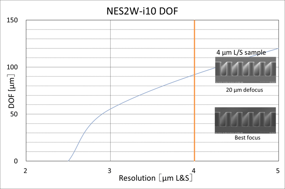
The NES2W-i10 stepper delivers tremendous depth of focus.
