- Home
- About Us
- Products and Technology
- Support and Training
Deliver i-line capabilities with resolution ≤ 1 µm
Nikon recognizes that i-line requirements are becoming increasingly prevalent, and NES1W-i04 steppers accommodate i-line resist processing and deliver resolution capabilities below 1 µm, with champion data down to 0.8 µm demonstrated. These MEMS steppers utilize a 0.12 to 0.24 variable numerical aperture projection lens design with 2.5x reduction that was developed to address the unique process challenges presented by these specialized i-line applications. The NES1W-i04 enables up to 6 µm depth of focus, and its advanced autofocus system provides die-by-die autofocus capabilities that further increase yield for these challenging processes. NES1W-i04 systems fully satisfy the diverse and ever-changing requirements for MEMS i-line research and development applications.
Deliver excellent overlay performance
Problematic effects such as wafer deformation and process-induced shrinkage can be challenging for some applications; however, the Nikon NES1W-i04 employs enhanced global alignment (EGA) to optimize overlay accuracy to 0.30 µm for the 15 mm field. EGA functions by utilizing multiple alignment marks across the wafer to ensure best fit alignment and thereby compensate for rotation issues or process-induced deformations. Pattern Matching Alignment capabilities are also available to provide increased flexibility for reticle design.
Support backside alignment to 0.8 µm
Customers may also choose to add on backside alignment functionality to enable precise alignment of 0.8 µm and below to marks located on the backside of the wafer surface. The industry-leading backside alignment system incorporates both direct and infra-red alignment capabilities to optimize performance.
Provides optimal productivity and fab efficiency
NES1W-i04 steppers can process up to 62 150 mm wafers per hour, and the substrate handling system employs a newly developed edge grip design that works well with TAIKO® and other thin wafers, and the verneuil chuck can utilize non-contact delivery as well as traditional handling. The chuck design also enables dual-sided non-contact exposure.
In addition, NES1W-i04 steppers reduce reticle costs with the Dual Exposure Area for a Single Reticle function, which makes it possible to utilize two separate exposure patterns on a single reticle by rotating the reticle according to programmable settings. Reticle blinds are then used to control the actual exposure area. In addition to delivering productivity benefits to ensure low cost of ownership for manufacturers, these steppers also minimize total fab costs with compact footprints, and satisfy global safety compliance specifications.
| Wavelength (nm) | 365 |
| Lens-NA | 0.12 – 0.24 variable |
| Exposure Area (mm) | 15 mm square |
| Reduction Ratio | 1/2.5 |
| Resolution (µm) | 1.0 |
| Depth of Focus (µm) | 6.0 |
| Overlay Accuracy (µm) | 0.30 |
| Throughput | 150 mm: 62 WPH |
| Wafer Size (mm) | ≤ 150 |
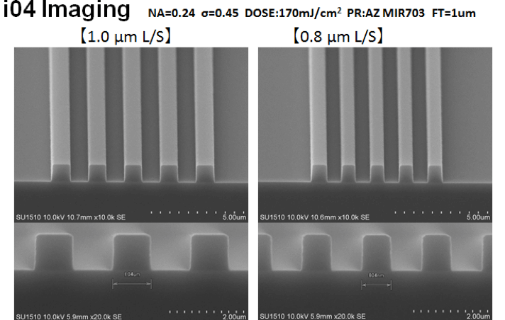
Resolution below 1 µm with newly developed i04 projection lens.
