- Home
- About Us
- Products and Technology
- Support and Training
In addition to delivering steppers and scanners for cutting-edge semiconductor applications, Nikon also offers a suite of advanced semiconductor inspection systems. Nikon leverages over 100 years of optical design and manufacturing expertise to deliver inspection systems to meet the most challenging post-develop and post-etch inspection requirements of today’s IC makers. Nikon also provides specialized illumination systems for image sensor inspection.
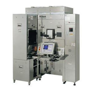
Systems provide advanced micro/macro inspection capabilities.

Provide high throughput inspection of entire wafer surface.
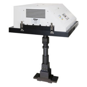
Deliver high-power, ultra-uniform illumination over a large inspection field.