- Home
- About Us
- Products and Technology
- Support and Training
Although MEMS do not have the same aggressive requirements for imaging or overlay capabilities that are demanded by semiconductors, they necessitate that the lithography systems are able to handle extremely warped wafers and very thick films, and accommodate significant step heights with reasonable overlay accuracy. In addition, bulk MEMS applications, Taiko-processed or bonded thin wafers often need precise alignment to marks located on the backside of the wafer surface. Nikon MEMS Steppers fully satisfy the critical requirements of these dynamic markets, and nearly 200 systems are in use by customers around the world today.
Nikon offers a variety of MEMS Steppers that accommodate ghi and i-line resist processes, which are becoming increasingly prevalent in MEMS manufacturing. Proven stepper technology ensures optimal CD uniformity across the wafer and projection lens designs eliminate costly mask contamination/defectivity issues experienced with contact or proximity printing methods. In addition, all Nikon MEMS Steppers utilize Enhanced Global Alignment (EGA) that has long been employed on traditional Nikon Step and Repeat Systems to provide optimal overlay accuracy. They also provide Pattern Matching Alignment capabilities that enable alignment using structures other than specific alignment marks. These critical functions are delivered on user-friendly, high productivity stepper platforms, with dramatically reduced system footprints to minimize equipment cost and cleanroom floor space usage.
Nikon continues to focus on expanding system capabilities and reducing cost to customers. Current stepper offerings enable field sizes up to 44 x 44 mm, and support a variety of substrate types and dimensions. They also deliver enhanced imaging and maximize productivity. Additionally, a multitude of add-on functions further boost MEMS Stepper performance and yield.
Nikon provides a comprehensive equipment portfolio, enabling improved time to market and return on investment for our customers.

Delivers i-line research and development capabilities with resolution ≤ 1.0 µm.
Provides 22 mm² field size and ≤ 1.2 µm resolution for leading-edge MEMS applications.

Deliver ghi-line capabilities with resolution ≤ 2.5 µm. Targeted for MEMS, IC backend layers, and power device applications.
Deliver i-line capabilities with resolution ≤ 2.0 µm for discrete, power, and analog device processing.

Delivers tremendous depth of focus and 44 mm² field size.
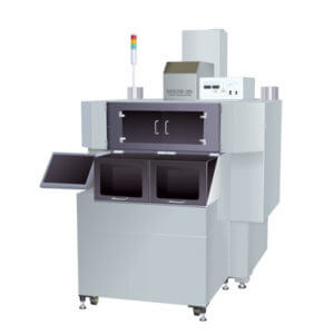
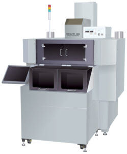
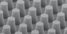 Nikon continues to expand the MEMS Stepper product line to satisfy the unique photolithography requirements of Air Bearing Surface (ABS) fabrication for magnetic heads, Micro Electro Mechanical Systems (MEMS) and Light Emitting Diodes (LED). These steppers are also used in back-end processing, as well as optoelectronics, discrete semiconductors and crystal oscillator manufacturing. These specialized Nikon lithography solutions deliver maximum stepper yield at the lowest possible cost.