- Home
- About Us
- Products and Technology
- Support and Training
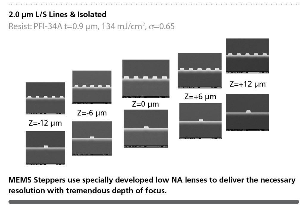
Deliver i-line capabilities with resolution ≤ 2 µm
Nikon recognizes that i-line applications are becoming increasingly prevalent, and the NES1W-i06/NES2W-i06 steppers accommodate i-line resist processing and deliver resolution capabilities below 2 µm. Champion data down to 1.4 µm has been demonstrated as well. The NES1W-i06/NES2W-i06 systems fully satisfy the diverse and ever-changing requirements for discrete, power and analog device processing.
Accommodate challenging process requirements with 22 µm depth of focus
These MEMS steppers utilize a 0.13 numerical aperture projection lens design with 1.8x reduction that was developed to address the unique process challenges presented by these specialized i-line applications. The NES1W-i06/NES2W-i06 systems enable up to 22 µm depth of focus, and their advanced autofocus systems provide die-by-die autofocus capabilities that further increase yield for these difficult processes.
Enhance mix and match with NSR steppers using 22 mm field size
The NES1W-i06/NES2W-i06 make use of advanced lens technology to enable the same 22 mm x 22 mm exposure field as traditional 5x reduction steppers, simplifying mix-and-match applications while boosting productivity. To further simply matching and reticle design, it is also possible to use the same alignment marks (FIA X/Y simultaneous marks) on these systems as on traditional NSR steppers.
Deliver excellent overlay performance for large field
Problematic effects such as wafer deformation and process-induced shrinkage can be challenging for some applications; however, the NES1W-i06 and NES2W-i06 employ enhanced global alignment (EGA) to optimize overlay accuracy to 0.30 and 0.35 µm respectively for the large 22 mm field. EGA functions by utilizing multiple alignment marks across the wafer to ensure best fit alignment and thereby compensate for rotation issues or process-induced deformations. Pattern Matching Alignment capabilities are also available to provide increased flexibility for reticle design.
Support backside alignment to 0.8 µm
Customers may also choose to add on backside alignment functionality to enable precise alignment of 0.8 µm and below to marks located on the backside of the wafer surface. The newly developed backside alignment system incorporates both direct and infra-red alignment capabilities to optimize performance.
| Wavelength (nm) | 365 |
| Lens-NA | 0.13 |
| Exposure Area (mm) | 22 mm square to 17.9 (H) x 25.2 (V) mm |
| Reduction Ratio | 1/1.8 |
| Resolution (µm) | 2.0 |
| Depth of Focus (µm) | 22 |
| Overlay Accuracy (µm) | NES1W-i06: 0.30 NES2W-i06: 0.35 |
| Throughput | NES1W-i06: 150 mm – 82 WPH NES2W-i06: 200 mm – 45 WPH |
| Wafer Size (mm) | NES1W-i06: ≤ 150 NES2W-i06: 150 and 200 |