Supports a variety of semiconductor devices and integrates well with existing fab equipment and operations
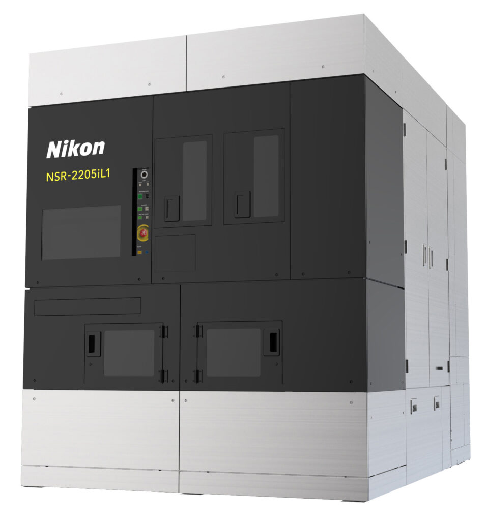
Tokyo, Japan – August 31, 2023 – Nikon Corporation is pleased to announce the release of the NSR-2205iL1 5x reduction i-line stepper, which was developed to manufacture a variety of devices including power and communications semiconductors, and Micro Electro Mechanical Systems (MEMS). In addition, the 2205iL1 stepper is compatible with existing Nikon i-line exposure systems and can be readily integrated with a fab’s current equipment and operations. This novel i-line lithography system builds upon decades of Nikon stepper innovations and expertise to deliver excellent affordability and productivity for semiconductor devices, regardless of the wafer substrate material. Orders are being accepted now, and sales of the NSR-2205iL1 will begin summer of 2024.
As electric vehicles, high-speed communications and various IT devices become more pervasive, demand for the semiconductors that support them continues to grow. These semiconductors must perform a variety of challenging functions, and as result, device makers require specialized substrates and exposure systems to manufacture those chips. To satisfy these current and future production needs, Nikon partnered closely with customers in developing the NSR-2205iL1 to meet their specific 5x i-line stepper requirements.
The NSR-2205iL1 leverages well-established Nikon technologies to deliver high stepper productivity with maximized yield across varying manufacturing processes. This includes high-accuracy wafer measurement using multipoint autofocus (AF), advanced wafer stage leveling*1, and large depth of focus (DOF) to maximize process window, among other central benefits. The 2205iL1 also accommodates a multitude of applications through compatibility with different wafer sizes and thicknesses, has high wafer warpage tolerance, and supports customers’ varied production applications including SiC (silicon carbide) and GaN (gallium nitride) processes.
In addition to optimizing manufacturing flexibility and affordability for device makers, the 2205iL1 was designed to be readily integrated with existing fab equipment and operations. Customers already having Nikon i-line exposure systems can utilize their current photomasks and wafer exposure recipes, and the NSR-2205iL1 can supplement or replace existing steppers that no longer meet manufacturing requirements. The 2250i1L1 was also developed with a focus on sustainability and future maintenance, and many previously custom-type components were transitioned to general-purpose commercially available ones to reduce supply chain challenges.
Nikon continues to expand its lithography equipment portfolio, and the NSR-2205iL1 builds upon vast Nikon stepper experience to deliver a flexible, cost-effective, and sustainable solution to fully satisfy customers’ current and long-term i-line processing objectives.
NSR-2205iL1 5x Reduction i-Line Stepper
System Overview
| Resolution (nm) | ≤ 350 nm (*2) |
| Lens-NA (numerical aperture) | 0.45 |
| Wavelength | 365 nm |
| Reduction ratio | 1:5 |
| Maximum exposure area | 22 mm x 22 mm |
| Overlay accuracy | SMO *3: ≤ 70 nm*2 |
*1 Mechanism that corrects the shift between the exposure image plane and the substrate surface during exposure by tilting the platform (stage) on which the wafer is placed.
*2 Annular; precision mode
*3 SMO (Single Machine Overlay): Overlay accuracy on the same NSR
The information contained in this press release is current as of its date of publication.
About Nikon
Since 1980, Nikon Corporation has been revolutionizing lithography with innovative products and technologies. The company is a worldwide leader in semiconductor lithography systems for the microelectronics manufacturing industry with more than 8,000 (semiconductor) lithography systems installed worldwide. Nikon offers the most extensive selection of production-class steppers and scanners in the industry. These products serve the semiconductor, flat panel display (FPD) and thin-film magnetic head (TFH) industries. Nikon Precision Inc. provides service, training, applications and technical support, as well as sales and marketing for Nikon lithography equipment in North America. For more information about Nikon, access our website at https://www.nikonprecision.com.
####
This press release contains forward-looking statements as that term is defined in the Private Securities Reform Act of 1995, which are subject to known and unknown risks and uncertainties that could cause actual results to differ materially from those expressed or implied by such statements. Such statements are subject to risks, uncertainties and changes in condition, particularly those related to industry requirements and other risks. The Company undertakes no obligation to update the information in this press release.
For further information, contact:
Holly Magoon, Senior Marketing Manager
Nikon Precision Inc.
holly.magoon@nikon.com