- Home
- About Us
- Products and Technology
- Support and Training
Accelerating Innovation in Logic, Memory, and Image Sensors
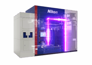
As the rise of IoT and AI accelerates, the demand for ever smaller, higher-performance semiconductor devices increases. From advanced logic chips to next-generation memory and high-resolution image sensors, manufacturers are under increasing pressure to achieve tighter overlay accuracy and higher productivity. To meet these demands, Nikon developed the NSR-S333F Dry ArF Scanner to deliver exceptional productivity with precision accuracy. Offering ≤ 65 nm resolution and a 0.92 NA, the S333F supports the imaging requirements of cutting-edge logic, DRAM, SRAM, and high-resolution image sensor devices.
High Productivity Meets Precision Overlay
The NSR-S333F is Nikon’s next-generation Dry ArF scanner, engineered for exceptional throughput and industry-leading overlay accuracy. The S333F achieves ≥ 300 wafers/hour (96 shots) by leveraging the stage speed and system architecture of Nikon’s advanced ArF immersion platform. This enables fabs to ramp faster, maximize tool utilization, and reduce cycle time. With improved stage control, enhanced metrology, and updated optical alignment systems, the S333F delivers ≤ 4 nm mix-and-match overlay (MMO) essential for advanced multi-patterning and high-density device fabrication.
Proven Optical Technology
Built on Nikon’s trusted ArF optics and leveraging the flagship immersion platform of the S636E, the S333F ensures stable imaging performance during long production runs. It also offers dependable pattern fidelity with a 193 nm ArF excimer laser and 1:4 reduction dry-optical design.
Streamlign™ Platform Advantages
Since 2008, Nikon’s Streamlign™ platform has set the standard for precision and productivity. Key innovations include:
Designed for Today’s Scaling Challenges
The NSR-S333F Dry ArF Scanner addresses the demands of AI, data-centric computing, mobile scaling, and IoT growth with:
Experience Next-Generation Dry ArF Performance
Accelerate output, improve patterning accuracy, and maintain competitive yields with the NSR-S333 Dry ArF Scanner.
Contact Nikon Precision to learn more about how the S333F Dry ArF Scanner can support your manufacturing roadmap.
Read the full announcement behind the new S333 Dry ArF Scanner at: Nikon Launches New Dry ArF Scanner for Fine Pattering Across Logic, Memory, and Sensors.
| Resolution | ≦ 65 nm |
| NA (numerical aperture) | 0.92 |
| Light Source | ArF excimer laser (193 nm wavelength) |
| Reduction Ratio | 1 : 4 |
| Maximum Exposure Area | 26 mm x 33 mm |
| Overlay Accuracy | MMO: ≦ 4 nm |
| Throughput | ≧ 300 wafers / hour (96 shots) |