Enables batch inspection and measurement across entire 300 mm wafer area
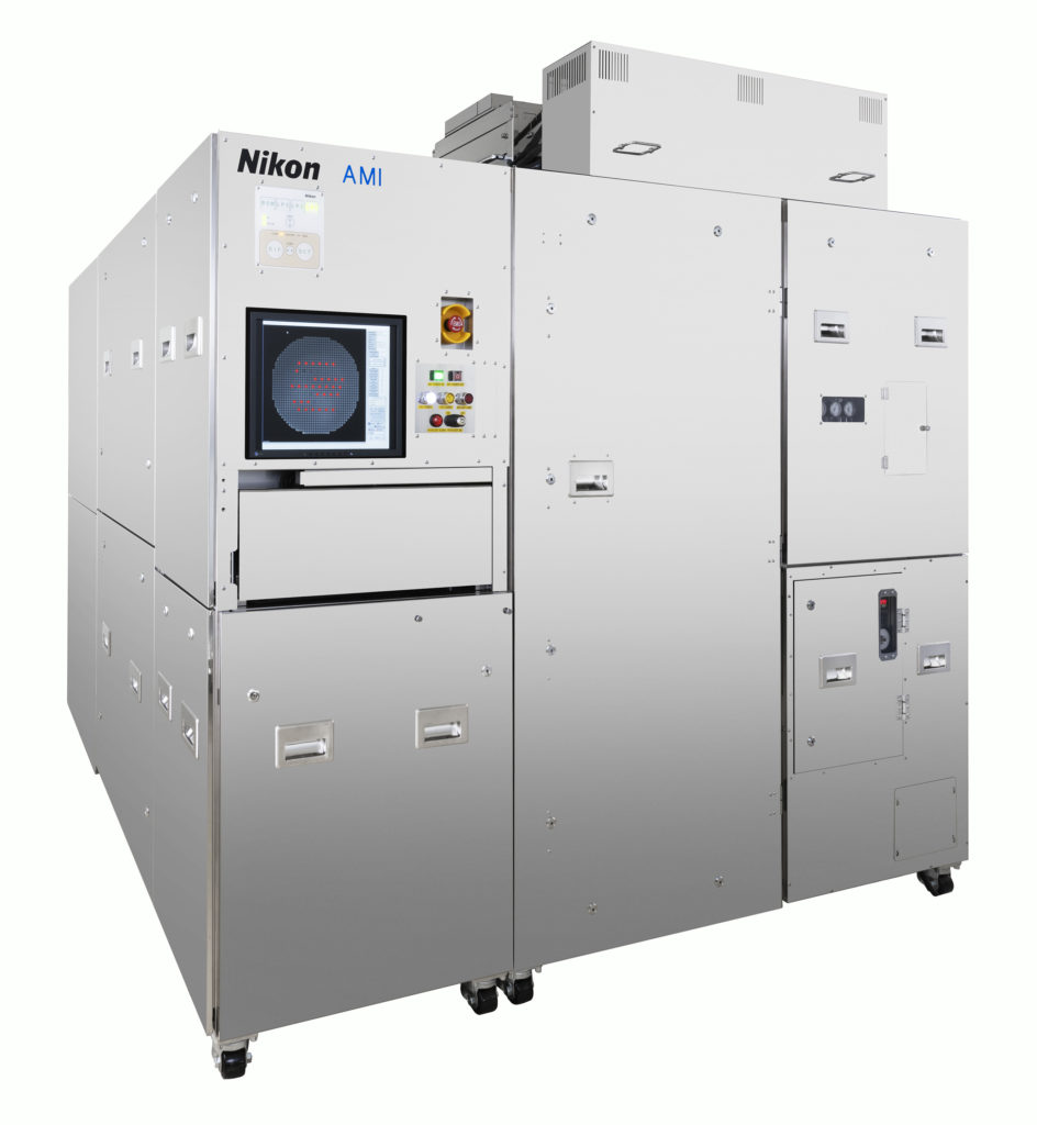
Tokyo, Japan – October 21, 2021 – Nikon Corporation (President: Toshikazu Umatate, Minato-ku, Tokyo) is pleased to announce the upcoming release of the AMI-5700 automatic macro inspection system, which performs batch inspection of 300 mm wafers with exceptional sensitivity and maximized productivity.
Nikon automatic macro inspection equipment (the AMI series) are inspection systems that detect semiconductor wafer defects, and the industry-leading AMI-5700 provides ultra-fine sensitivity and superior throughput using simultaneous capture of images across the entire wafer. Many AMI systems are operating in 300 mm wafer manufacturing facilities worldwide, contributing to early detection of wafer defects that can occur in semiconductor mass production processes.
Like previous-generation AMI systems, the AMI-5700 (to be released in early November 2021) delivers very efficient, advanced inspection capabilities. The leading-edge AMI-5700 is not limited to wafer inspection though, it can also measure the wafer and detect defects. In addition to performing 180 wafers per hour (300 mm full wafer) inspection, a newly developed optional high-speed measurement function enables the AMI-5700 to also measure pattern linewidth, coating thickness, and focus at a rate of 100,000 or more points/min (Note 1). The AMI-5700 also features 3 load ports for wafer carriers to reduce transfer wait time in the fab and increase production efficiency. The AMI-5700 helps users better manage their semiconductor device production processes and boosts productivity of their semiconductor fabs.
The 5700 also features newly developed optics and an enhanced condensed mirror that enable high-quality image capture with low chromatic aberration. The AMI-5700 detects errors greater than or equal to ±10% of the target pattern sizes: 22 nm for lines/spaces, 50 nm for holes (Note 2) and 80 nm for spaces using diffraction inspection. In addition, the innovative scatter inspection unit enables exceptional detection sensitivity, with the AMI-5700 capable of detecting particles and scratches as small as 5 µm compared to 15 µm using earlier models.
Nikon is committed to providing industry-leading inspection solutions like the AMI-5700 that enable customers to advance semiconductor manufacturing and support the digital transformation.
Note 1: This data is obtained when batch image capturing is performed 3 times under different conditions at a minimum exposure time.
Note 2: Circular opening connecting the layer on which circuit elements are formed to a layer for wiring, or one connecting between layers for multilayer metal wiring.
Body Specifications
| Dimensions (W x D x H) | 2,362 mm × 2,420 mm |
| Weight | Approx. 2,600 kg (with the scatter inspection and backside inspection options) |
The information contained in this press release is current as of its date of publication.
About Nikon
Since 1980, Nikon Corporation has been revolutionizing lithography with innovative products and technologies. The company is a worldwide leader in semiconductor lithography systems for the microelectronics manufacturing industry with more than 8,000 (semiconductor) lithography systems installed worldwide. Nikon offers the most extensive selection of production-class steppers and scanners in the industry. These products serve the semiconductor, flat panel display (FPD) and thin-film magnetic head (TFH) industries. Nikon Precision Inc. provides service, training, applications and technical support, as well as sales and marketing for Nikon lithography equipment in North America. For more information about Nikon, access our website at https://www.nikonprecision.com.
####
This press release contains forward-looking statements as that term is defined in the Private Securities Reform Act of 1995, which are subject to known and unknown risks and uncertainties that could cause actual results to differ materially from those expressed or implied by such statements. Such statements are subject to risks, uncertainties and changes in condition, particularly those related to industry requirements and other risks. The Company undertakes no obligation to update the information in this press release.
For further information, contact:
Holly Magoon, Senior Marketing Manager
Nikon Precision Inc.
holly.magoon@nikon.com