Provides world-class device patterning and productivity for cutting-edge semiconductor manufacturing
Logic devices push leading-edge scaling requirements due to their many critical layers and complex multi-patterning process steps. Edge Placement Error (EPE) is the main challenge for these devices, and the key requirement for ArFi extension is stringent on-product overlay (OPO) control. In addition to scanner contributors, a major component of the OPO error budget is process-induced wafer grid errors. Therefore, Nikon has been aggressively developing new technologies targeting both scanner and process-related OPO error factors.
The industry-leading NSR-S635E ArF immersion scanner leverages the well-known Streamlign platform. It incorporates the latest developments in lens, autofocus, alignment, and defectivity minimization technology to deliver unparalleled multiple patterning performance and productivity. The S635E is integrated with the pioneering inline Alignment Station (iAS), and is compatible with sophisticated computational and on-product learning software solutions. Together, these elements ensure world-class device patterning and optimum fab productivity to fully satisfy cutting-edge semiconductor manufacturing requirements.
Delivers improved on-product overlay performance to satisfy stringent edge placement requirements for multiple patterning
The NSR-S635E utilizes the established Bird’s Eye Control system to accurately determine wafer position and a reticle stage with an encoder servo system to increase accuracy. Enhancements to the scanner’s stage controller and metrology system enable superior overlay accuracy, while expanded temperature control capabilities and optimized component materials ensure superior tool overlay stability, even under the most extreme production conditions.
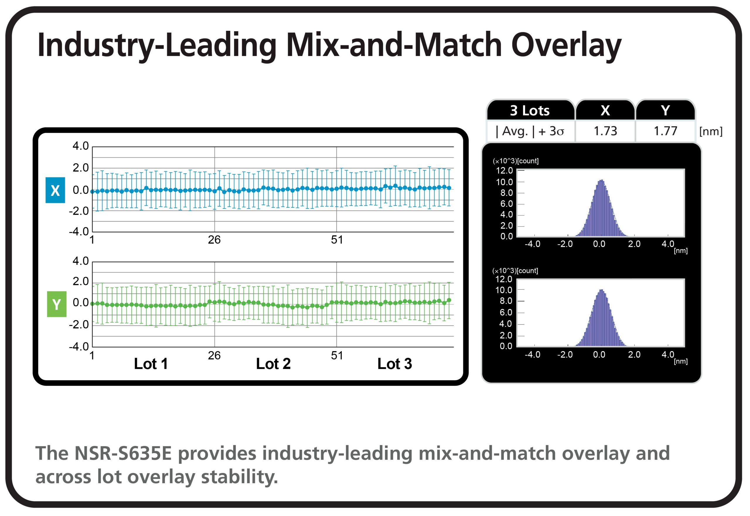
The S635E also supports Dynamic Matching Adjustment control functions to expand overlay matching capabilities, and is integrated with the Nikon inline alignment station (iAS) to further enhance scanner on-product overlay performance and productivity. These cutting-edge technologies are a significant factor in overlay and matching performance for multiple patterning applications. The S635E has demonstrated excellent mix-and-match overlay (Avg. +3σ) performance below 1.8 nm across 3 lots.
Ensures excellent focus stability and minimizes defects to enhance yield
Advances in scaling inevitably come with reduced depth of focus, while focus variation can lead to increased CD variation and thus increased edge placement error. As a result, the focus budget is as critical as the overlay budget at leading-edge nodes. The S635E autofocus (AF) system reduces variability for product materials. It enables exceptional focus control with a best mean focus range of 4.4 nm and across wafer uniformity of 7.3 nm (3σ) across a one week period using phase shift focus monitor (PSFM). This satisfies autofocus requirements of current and future nodes.
Defectivity is another crucial parameter for advanced logic patterning. Increasing ArF immersion layers and non-redundancy in logic circuits drive increasingly demanding defectivity specifications. However, faster litho tool scan speeds can induce more droplets and add defects, while different products’ shot layouts have distinct exposure motions that result in varied immersion water behavior. In addition to employing a low defectivity nozzle design, the S635E enables innovative computational defectivity corrections. By considering the shot map and scanner settings, the S635E predicts the defectivity behavior. It then modifies the scanning motions and optimizes the exposure tool recipe to reduce defects while also delivering ultra-high throughput.
Enables sophisticated computational and on-product learning solutions
The NSR-S635E is also compatible with a number of automated software solutions that ensure the scanner is performing at its best. CDU Simulator provides high-order dose and focus adjustments to reduce residual CD errors from sources including mask, etch, and the litho process. OPE Optimizer uses customer test-pattern data and scanner adjustments to provide illumination condition matching for aligning performance across a fleet of scanners. The NSR-S635E supports Zeroing XY, AF, and DIS functions to optimize performance stability as well. These various tuning functions deliver optimized scanner/exposure parameters that increase yield in high volume manufacturing.
Optimizes affordability with ultra-high throughput up to 275 wafers per hour
Affordability is a vital parameter for immersion multiple patterning. NSR-S635E reliability and throughput are critical factors in boosting wafer output per day and overall cost efficiency. The NSR-S635E can process up to 275 wafers per hour using a scan speed of 900 mm/sec and a 120 watt laser. In addition, nozzle innovations prevent immersion defects, while enhanced overlay and focus stability contribute to maximized tool productivity and fab daily output. These are all crucial factors in enabling cost-effective, leading-edge multiple patterning.
Immersion lithography and multiple patterning play pivotal roles in current and future generations of IC manufacturing. The S635E delivers exceptional manufacturing performance and productivity—now and for the future.
| Wavelength (nm) | 193 |
| Lens-NA | 1.35 |
| Exposure Area (mm) | 26 x 33 |
| Reduction Ratio | 1/4 |
| Resolution (nm) | ≤ 38 |
| Mix-and-Match Overlay (nm) | ≤ 2.1 |
| Throughput: | |
| 300 mm (96 exp fields) | ≥ 275 |
| Wafer Size (mm) | 300 |