Advanced solution for critical layers, and supports 3D semiconductor device production
Tokyo, Japan – December 6, 2023 – Nikon Corporation (Nikon) is pleased to announce the release of the NSR-S636E ArF immersion scanner, with system sales launching in January 2024. With the highest productivity of any lithography system across the impressive history of Nikon, the NSR-S636E is an immersion lithography scanner for critical layers that delivers superior overlay accuracy and ultra-high throughput. The NSR-S636E is the optimum patterning solution for the many diverse structures used in cutting-edge semiconductors, including 3D devices.
As the digital transformation accelerates, high-performance semiconductors that can process and transmit larger amounts of data more quickly are becoming increasingly critical. The key enablers in technology innovation for leading-edge semiconductor performance are circuit pattern miniaturization as well as 3D semiconductor device structures, and ArF immersion scanners are essential for both of these manufacturing processes. When compared to conventional semiconductor processing, wafer warpage and distortions are more likely to occur during 3D semiconductor manufacturing, necessitating even more advanced scanner correction and compensation capabilities than ever before.
The NSR-S636E ArF immersion scanner utilizes an enhanced iAS*1 that performs sophisticated wafer multipoint measurement before exposure. This innovative system delivers next-level overlay accuracy using high-precision measurement and extensive wafer warpage and distortion correction capabilities, all while maintaining maximum scanner throughput. Overall scanner output is also 10-15% higher*2 than current generation systems, resulting in optimized efficiency in cutting-edge semiconductor device production.
The S636E immersion lithography system delivers excellent performance across diverse production processes including 3D-ICs where wafer deformation can easily occur. Enhanced accuracy of the iAS that performs wafer multipoint measurement before exposure enables heightened accuracy in measuring deformations such as wafer warping and distortion. Advanced measurement and compensation capabilities improve process robustness and provide superior overlay performance, without impacting productivity. These innovations are vital to diverse manufacturing processes such as 3D-ICs that require ultra-high overlay accuracy and will continue to be developed to achieve unprecedented semiconductor performance. In addition, through comprehensive improvements in throughput and daily productivity optimization, the NSR-S636E ArF immersion scanner also boosts overall output by 10-15% compared to current models. This is the highest level of productivity across the entire history of Nikon semiconductor lithography systems.
Nikon continues to provide invaluable solutions like the NSR-S636E for leading IC production and to support the development of our digital society. We are committed to continuing to push the limits of photolithography through industry-leading solutions such as the S636E to support our customers’ manufacturing objectives for many years to come.
*1 Abbreviation of inline Alignment Station. This system measures wafers with high speed and accuracy and enables grid error correction without reducing exposure system throughput.
*2 This can vary depending on usage conditions and other factors.
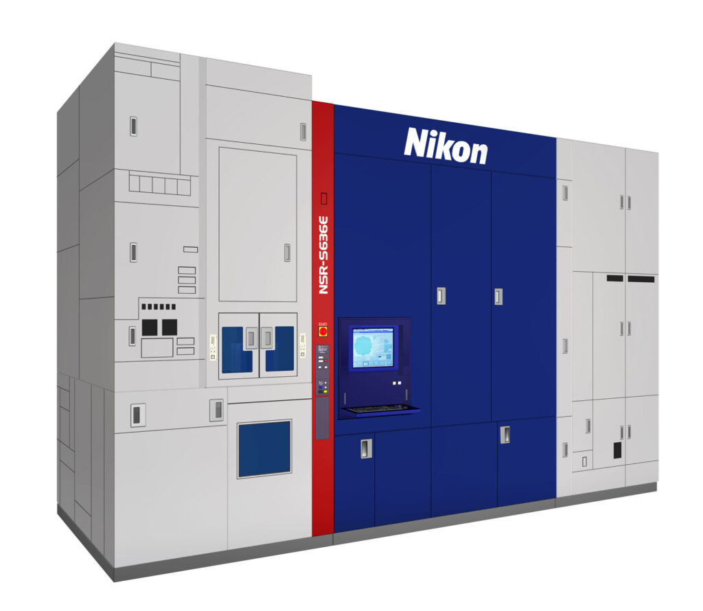
Nikon NSR-S636E ArF Immersion Scanner
System Overview
| Resolution | ≤ 38 nm |
| Lens-NA (numerical aperture) | 1.35 |
| Wavelength | ArF 193 nm |
| Reduction ratio | 1:4 |
| Maximum exposure area | 26 mm x 33 mm |
| Overlay Accuracy | MMO*3: ≤ 2.1 nm |
| Throughput | ≥280 wafers/hour (96 shots) |
The information contained in this press release is current as of its date of publication.
About Nikon
Since 1980, Nikon Corporation has been revolutionizing lithography with innovative products and technologies. The company is a worldwide leader in semiconductor lithography systems for the microelectronics manufacturing industry with more than 8,000 (semiconductor) lithography systems installed worldwide. Nikon offers the most extensive selection of production-class steppers and scanners in the industry. These products serve the semiconductor, flat panel display (FPD) and thin-film magnetic head (TFH) industries. Nikon Precision Inc. provides service, training, applications and technical support, as well as sales and marketing for Nikon lithography equipment in North America. For more information about Nikon, access our website at https://www.nikonprecision.com.
####
This press release contains forward-looking statements as that term is defined in the Private Securities Reform Act of 1995, which are subject to known and unknown risks and uncertainties that could cause actual results to differ materially from those expressed or implied by such statements. Such statements are subject to risks, uncertainties and changes in condition, particularly those related to industry requirements and other risks. The Company undertakes no obligation to update the information in this press release.
For further information, please contact:
Nikon Precision Marketing Communications at:
NPIcom@nikon.com